I2C (Inter Integrated Circuit Communication)
I2C – Inter-Integrated Circuit Communication is a widely used protocol for communication between modules of a digital systems both inside a chip as well as on a circuit board. Operating on two frequencies 100 MHz and 400 MHz, I2C is categorized as a slow mode of communication but widely useful in interconnecting slow speed peripherals to processor systems and embedded systems due to its simplicity and efficiency. With the wide spread of IOT and embedded systems, this communication protocol has become and integral part of modern day electronics.
I2C protocol makes use of two bi-directional open drain lines for which it is also dubbed the ‘Two wire communication’. The two bi directional buses are,
- Serial Data Line (SDA)
- Serial Clock Line (SCL)
These two buses are pulled up by all the devices connecting them to either 5V or 3.3V depending on the operating voltage of the system. All the devices or peripherals using the I2C protocol for communication in a circuit are connected to the same two buses and the protocol assigns unique ID’s for each device. Any of the devices can initiate a communication with another and the node initiating the communication becomes the master while the other becomes the slave.
The master signals the start of a communication by starting a clock signal in SCL and sending a start bit (start bit is a high-to-low transactio of SDA with the SCL high) followed by a 7 bit address of the expected slave in the SDA. All the other nodes connected to these two lines recieve the signal but only the node whose address matches with the broadcasted address responds to the master with an ACK bit. A master node can both send and recieve data from another node which means a node can be in four modes of operation.
- Master transmit – master node is sending data to a slave
- Master receive – master node is receiving data from a slave
- Slave transmit – slave node is sending data to the master
- Slave receive – slave node is receiving data from the master
Address and data are sent as monst significant bit first (MSB first) in all the transactions and each transaction should be acknowledge by the slave. Stop bit which is a low-to-high transition of the SDA with SCL high is sent to indicate a proper end of transaction.
The number of nodes that can be connected to a I2C network does not have have a limit other than the address constraint which limits the number of nodes to 2^7 = 128 because the addresses have only 7 bits. Since the operating clock speed is either 400MHz or 100MHz, I2C lines can be extended over a long distance up to about a meter without any issue. This enables connecting lot of peripherals to processing systems using the I2C communication.
Most of the modern IC’s that are commonly used in embedded systems and development boards require configuring using the I2C. For example, the HDMI transmitter IC ADV7511 in zynq 706 evaluation board requires configuring to the input mode for it to be able to tranmit HDMI video. Therefore either a micro controller or an FPGA on the evaluation board requires to act as an I2C master and configure the HDMI transmitter IC using I2C. Similar kind of sinarios are there in most of the modern day IC’s that we come across in most embedded systems.
The following diagram shows the I2C lines used for the communication among 5 devices.

Figure1: Bus architecture
Timing Diagram

Figure2: i2c timing diagram presented in Wikipedia
- S – Start condition – Master pulls SDA LOW while maintaining SCL HIGH
- P – Stop condition – Master pulls SDC HIGH while maintaining SCL HIGH
- B1…BN – Read condition – Master or Slave ( depends on who is transmitting ) read data when SCL is HIGH
- BLUE Bars – SDA is allowed to change when SCL is LOW. Only other scenarios where SDA changes when SCL is HIGH is when Start or Stop conditions are transmitted.
- After Start condition, first byte (8 bits) is the address frame
- First 7 bits of address frame is the slave address (up-to 127 slaves are allowed in 7bit addressing mode)
- Last bit is set to ‘1’ if Master is requesting data. It is ‘0’ if master is sending data.
- In the 9th cycle, addressed slave will pull SDA LOW to acknowledge. If the slave didn’t perform this Master can decide what to do next.
- After address frame, data frames are transmitted. Transmission completes when stop condition is transmitted.
- SCL is controlled by the master. However if the Slave is busy and not ready to transmit or receive data Slave will pull SCL LOW until it is ready. This is known as clock stretching. Once Slave is ready it will release SCL and Master will start clocking SCL signal.
Circuit Diagram

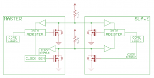
Circuit Diagram by Sparkfun i2c tutorial
Since both SDA and SCL are open drain (Set to HIGH when neither Master nor Slave is driving but either of them can pull it LOW) there will be no conflict in signaling. Additional benefit of I2C is ability to use for devices operating at different voltages(5v and 3.3v) without a level shifter (This can be done if lower operating voltage is considered logic HIGH by the device with higher operating voltage). In order to do this pull up resistor should be connected to the lower operating voltage.
Reference
[1] Sparkfun i2c tutorial : https://learn.sparkfun.com/tutorials/i2c
[2] Wikipedia : https://en.wikipedia.org/wiki/I²C

Leave a Reply