Himantha Alahakoon
Ripple Carry Adder
Basic gates such as NOT, OR, AND, NAND and NOR are used to carry out basic arithmetic operations like addition, subtraction, multiplication and division in processors. Addition is the most basic arithmetic operation, as subtraction (a series of negative addition), multiplication (a series of positive addition) and division (a series of negative addition) can be carried out as an extended operation of simple addition.
The simple adder module without carry in is called half adder and the adder with carry in is called full adder. Sample verilog code for a half adder and full adder can be found below.
1 2 3 4 5 6 7 8 9 10 11 12 13 14 15 16 17 18 19 | module half_adder( output S,Cout, input A,B ); assign S = A^B; assign Cout = A*B; endmodule module full_adder( output S,Cout, input A,B,Cin ); assign S = (A^B) ^ Cin; assign Cout = (A*B) | (A^B)*Cin; endmodule |
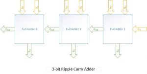
Multiple full adders can be cascaded in parallel to form a ‘N’ bit adder. The carry-out of a full adder is used as the carry-in of the succeeding full adder. Each of the carry bit gets rippled into the next stage, hence this adder is called the Ripple-carry-adder. Half-adder and Full-adder are the basic building blocks of the Ripple Adder. Below is the verilog implementation of a ripple adder.
1 2 3 4 5 6 7 8 9 10 11 12 | module ripple_adder( output reg [0:2] S, output reg Cout, input [0:2] A,B ); reg [0:1] c; half_adder F1(S[0], c[0], A[0], B[0]); full_adder F2(S[1], c[1], A[1], B[1], c[0]); full_adder F3(S[2], Cout, A[2], B[2], c[1]); endmodule |
The sum or carry out bits of a half adder stage is not valid until the carry in bit of that particular stage has occurred. For an example, S0 and Cout in the given diagram is not valid until Cin has taken place at the first stage. This is mainly governed by the propagation delay of the circuit. Hence the final result of the ripple adder would be valid only after the total propagation delay of the full adders involved. Suppose the propagation delay of an adder is T and there are n adders in the circuit. Hence the total propagation delay would be nT. The ultimate design goal would be to minimise this propagation delay.

Leave a Reply